High-Density Interconnect (HDI) PCB
Design & Capabilities


High-Density Interconnect (HDI) PCB
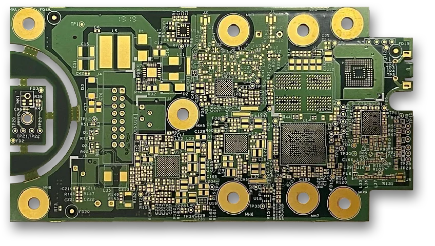
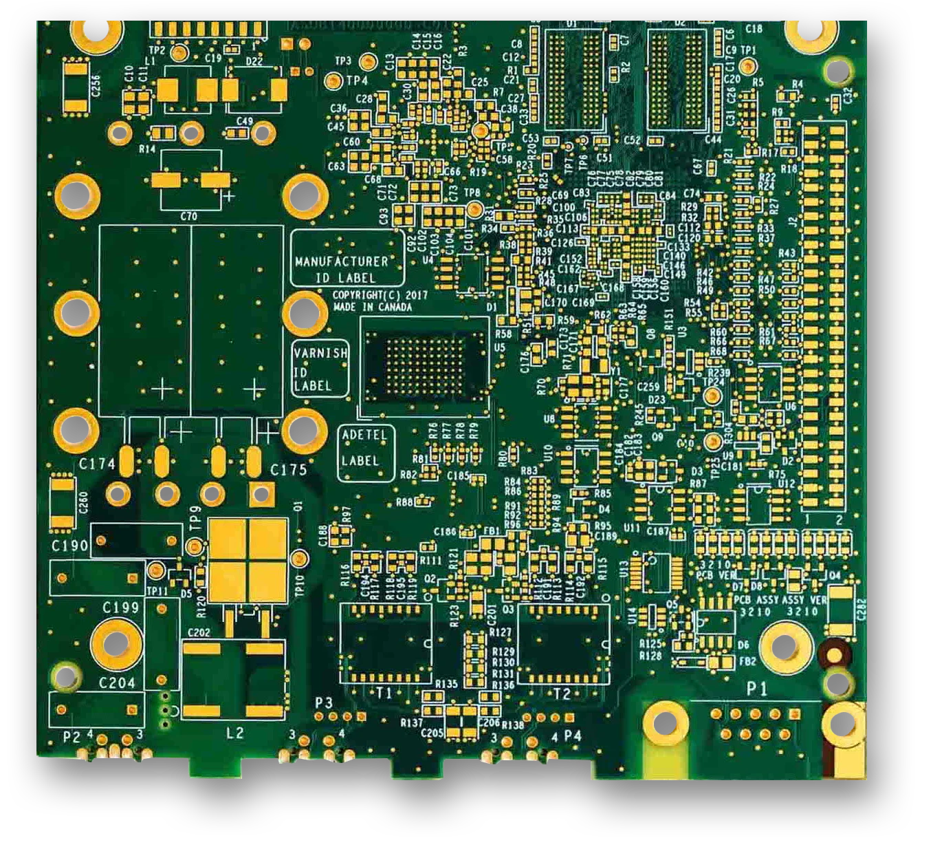
HDI PCB boards, one of the fastest growing technologies in the PCB industry. This types of PCB contain both the blind via and buried via hole varieties and have a higher circuitry density than traditional circuit boards. Hiberxen Electronics produces high quality HDI PCB with reliability.
HDI PCB stands for High-Density Interconnect Printed Circuit Board. These PCBs having relatively high circuit density that uses micro-blind and buried “via” or the copper-plated holes in PCB technology. These PCBs are compact product designed for small-capacity users, as they cost much more than standard PCB.
HDI PCB Advantages
HDI technology can reduce the ultimate cost of PCB.
- The traditional and complex pressing process is low.
- Increased circuit density: traditional circuit boards and parts are interconnected.
- Conducive to the use of advanced construction technology.
- Have better electrical performance and signal accuracy.
- Better reliability.
- Can improve thermal properties.
- Can improve radio frequency interference/electromagnetic wave interference/electrostatic discharge (RFI/EMI/ESD).
- Greater design efficiency.t
Types of HDI PCB
HDI PCB comes in different types with same functions. The type you decide to choose depends on the application you are using. Following are the different types of HDI PCBs.
- Rigid HDI PCB:
HDI PCBs are made of a solid and rigid substrate material such as fiberglass. This kind of material prevents the bending of the HDI board. The application of this HDI PCB can be found on towers of most desktops. - Rigid-Flex HDI PCB:
This is made of a rigid circuit board, which attaches to a flexible board. The design’s complexity depends on whatever application you are using. - Flex HDI PCB:
Flex HDI PCB is composed of flexible plastic. This material permits the board to form different shapes. This offers lots of benefits when compared with rigid boards. The board’s flexibility also allows you to move or bend easily during the process of application without bringing damage to the circuits that are present on the board. One disadvantage with this board type is that designing and manufacturing it costs a lot. However, they come with numerous benefits. The heavy wiring found in advanced equipment like satellites can be replaced with flexible HDI PCBs. They are lighter and make use of little space, making them great for such use. Another benefit is that it features different designs like multilayer, single-sided, or double-sided designs. - Multilayer HDI PCB:
These boards have substrate boards of multiple layers with an insulating material that separates these layers. Just like HDI PCBs with double sides, either vias or through holes can be used in connecting the board’s electric circuits. Multilayer HDI PCBs are very beneficial because they use less space. Standard applications using this HDI board type include medical machinery, servers, handheld devices, and computers.
- Rigid HDI PCB:
Rigid-Flex PCB Capabilities
| Item | Description | Remark | |
| Layer | 1- 32 Layers (FR- 4, FR- 406, 370 HR) 1- 2 Layers (Rogers, TEFLON) |
||
| Material | FR- 4, FR- 406, 370 HR; Rogers4003; Rogers4350 TEFLON |
||
| Finish Thickness | Finish Thickness: 0.008″ – 0.275″ (0.2mm- 7mm) | ||
| Min Thickness | 2- layer: 0.008″ (0.2mm) 4- layer: 0.016″ (0.4mm) 6- layer: 0.024″ (0.6mm) 8- layer: 0.032″ (0.8mm) 10- layer: 0.04″ (1mm) More than 10layers (0.5Xnumber of layers X0.008″) |
||
| Surface Finishing | Lead Finishing: HASL, HASL + Gold finger Lead- free Finishing: Lead- free HASL, ENG Gold; OSP, Immersion Silver |
||
| Special Process | Impedance board (request as±10%) High TG / Halogen- free/ Halogen- free & High TG board |
||
| Min Trace Width / Min Clearance |
Inner Layers (trace width/clearance) 0.5oz: 2.5/ 2.5mil 1oz: 3/ 3mil 2oz: 5/ 7mil 3oz: 7/ 8mil 4oz: 10/ 10mil 5oz: 12/ 12mil 6oz: 15/ 12mil |
Outer Layers (trace width/clearance) 1/ 3oz- Haz: 3/ 3mil 1oz: 3.5/ 3.5mil 2oz: 5/ 7mil 3oz: 7/ 8mil 4oz: 10/ 10mil 5oz: 12/ 12mil 6oz: 15/ 12mil |
|
| Aspect Ratio | Min Hole Size 6mil | ||
| Min Hole Ring |
Inner: 0.5oz: 4mil 1oz: 5mil 2oz: 6mil 3oz: 9mil 4oz: 12mil 5oz: 15mil 6oz: 17mil |
Outer: 1/ 3oz -0.5oz: 4mil 1oz: 4mil 2oz: 6mil 3oz: 9mil 4oz: 12mil 5oz: 15mil 6oz: 17mil |
|
| Copper Thickness | Inner: H0.5oz, 1oz, 2oz, 3oz, 4oz, 5oz. 6oz Outer: 1/ 3oz, 0.5oz, 1oz, 2oz, 3oz, 4oz, 5oz, 6oz |
||
| Min Hole Size and Tolerance | Min Finish Hole: 6mil Hole Tolerance: ±3mil |
||
| Thickness of Plating Layer |
· HASL: Copper Thickness: 20um -35um Tin 5 -20um · Immersion Gold: Nickel 100u” -200 u” Gold 2u” -4u” · Hard Plated Gold: Nickel 100u” -200 u” Gold 4u” -8u” · Golden Finger: Nickel : 100u” -200 u” Gold : 5u” -15u” · Immersion Silver: 6u” -12u” · OSP: Film 8u” -20u” |
||
| Solder Mask Color |
Glossy : Green, Black, Red, Yellow, White, Purple, Blue Matt : Green, Black |
||
| Solder Mask Resolution |
Solder Mask Thickness : 0.2mil -1.6mil Solder Dam : Green 7mil /Other Color 8mil Solder Mask Hole Plug Diameter : 10mil -25mil |
||
| Silk Screen Color | White, Black | ||
| Profile |
Punch Tol: ±5mil CNC Tol: ±5mil V- CUT Tol: ±10mil Bevel Edge: ±5mil Slot Min: 32mil Angel: 15°, 20°, 30°, 45°, 60° |
||
| Bow and Twist | SMT≤0.75% None SMT≤1% |
||
| Accept Standard | IPC Class 2; IPC Class 3; ISO9000 | ||
We're here to help
Our team is ready for you. Feel free to contact us by e-mail or our social media, so we can learn more about you and your needs.
