
You need a PCB layout software like Altium Designer to program a PCB board.
If you have ever built a circuit from a schematic, you know that it can be tedious work. But what if you could make your PCB board do the work for you? In this article, we will show you how to program a PCB board to automate the process of wiring your circuits.
First, you will need to purchase a PCB board. You can find these at most electronics stores or online. Make sure to get one that is the correct size for your project.
Next, you will need to gather the components for your circuit. Once you have all of the components, you will need to solder them to the PCB board. If you are not comfortable soldering, you can ask a friend or family member for help.
After the components are soldered to the PCB board, you will need to connect the power supply. Make sure to connect the positive lead to the positive voltage rail and the negative lead to the negative voltage rail.
Now, you will need to download a PCB design software. There are many different software programs available, but we recommend Eagle PCB. Once you have installed the software, you will need to open the project file for your PCB board.
Now, you will need to design your circuit. This can be done by adding components to the schematic editor and connecting them with wires. Once you have designed your circuit, you will need to generate a Gerber file. This file can be exported from Eagle PCB and sent to
How To Program A PCB Board?
You will need to use a PCB design program, such as Eagle, to design your PCB layout.

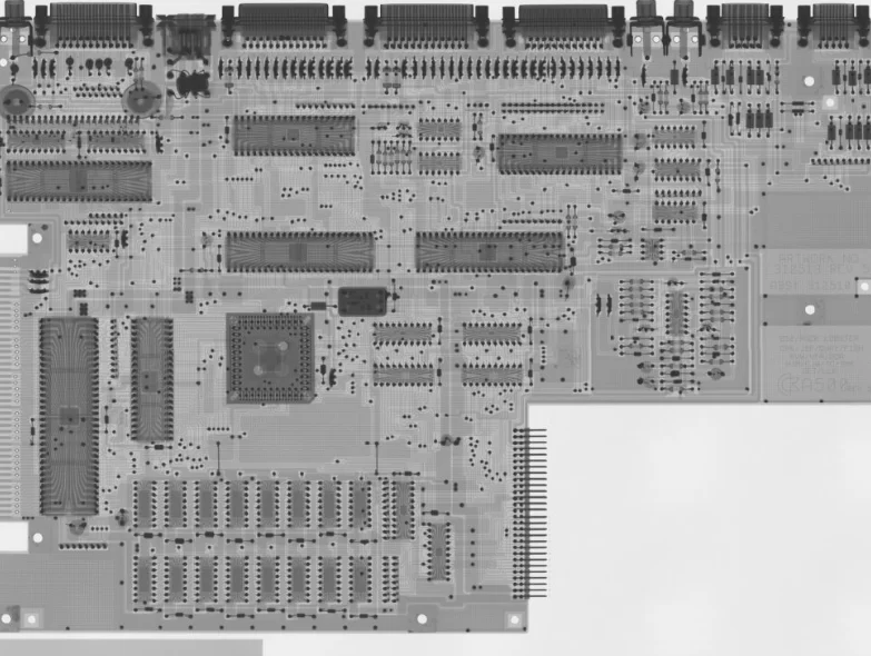
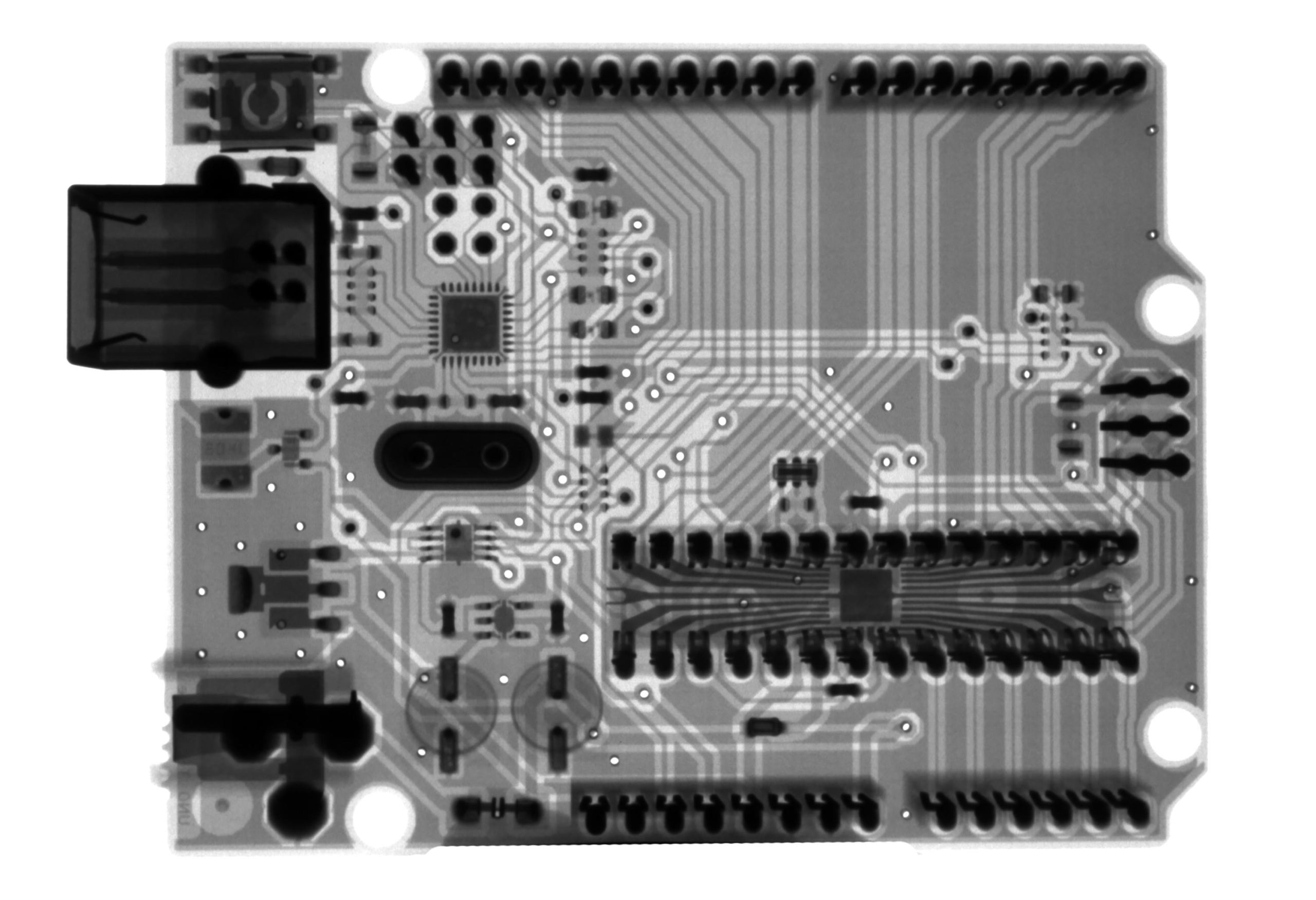
If you’ve ever wondered how those circuit boards inside your computer work, you’re not alone. Those little green (or sometimes blue) boards are called printed circuit boards, or PCBs, and they’re integral to just about every electronic device out there. Here’s a quick rundown on how they work and how they’re made.
A printed circuit board is made up of a few different layers. The substrate is the base layer, and it’s usually made of fiberglass or another type of insulation. On top of that is the copper layer, which is etched with the circuit design. Between the substrate and the copper layer is a layer of adhesive, which helps to hold everything together.
The circuit design is first created on a computer using a PCB design program. Once it’s been created, it’s sent to a machine that will etch the design onto the copper layer. Once that’s done, the adhesive layer is applied and the whole thing is cured in a special oven.
After the curing process is complete, the PCB is then cut to size and the various components are soldered onto it. These components can include things like resistors, capacitors, and transistors. Once everything is soldered on, the PCB is then tested to make sure that it works correctly.
PCBs are used in just about every electronic device out there, from your cell phone to your computer. They’re relatively simple to make, but they play a vital role in just about everything that uses electricity.
How To Design A PCB Board?
There is no one-size-fits-all answer to this question, as the design of a PCB board will vary depending on the specific requirements of the project. However, there are some general tips that can be followed when designing a PCB board, such as ensuring that the board has enough power and ground planes, using the right PCB stackup, and following the design guidelines for the chosen manufacturing process.
If you’re reading this, you’re probably wondering how to design a PCB board. Maybe you’re working on a new electronic device, or maybe you’re just curious about how it’s done. Either way, you’ve come to the right place.
PCB design is a complex process, but there are a few basic steps that anyone can follow to create a simple board. In this article, we’ll walk you through those steps and show you how to design a PCB board using our free online tool.
1. Choose your board shape and size
The first step in designing a PCB board is to choose the shape and size of your board. There are a few factors to consider here, such as the size of your components and the number of layers you need.
If you’re not sure what shape or size to choose, don’t worry – you can always change it later.
2. Add your components
The next step is to add your components to the board. You can do this by dragging and dropping them from the library onto the board.
If you’re not sure where to place a component, you can always use the autoroute feature to have the software figure it out for you.
3. Route your connections
Once all of your components are in place, you need to route the connections between them. This is called “tracing” and it’s usually done with a special kind of software.
If you’re using our online tool, you can route your connections by clicking on the “trace” button.
4. Review and order
The last step is to review your design and order your board. Once you’re happy with your design, you can send it to a manufacturer and they will create the board for you.
If you’re using our online tool, you can order your board directly from us. We’ll even give you a discount if you use the code “blog” at checkout.
That’s it! Those are the four basic steps to designing a PCB board. Of course, there are a lot of details that we didn’t cover here, but this should give you a good starting point.
If you want to learn more about PCB design, we recommend checking out our other blog articles or taking our free online course.
How To Etch A PCB Board?
To etch a PCB board, you need to use a chemical etching process.
If you’ve ever wanted to make a professional-looking PCB board at home, etching is the way to go. It’s not as hard as it sounds, and with a little practice you can produce high-quality boards.
First, you’ll need to gather your materials. You’ll need a PCB board, of course, and you’ll need a way to etch the board. You can use a chemical etchant or a CNC machine, but for this example we’ll use a simple chemical etchant. You’ll also need a way to transfer the design onto the board. You can use a pen or a laser printer, but the best way is to use a photoresist film.
Once you have your materials, it’s time to get started. Begin by cleaning the PCB board with isopropyl alcohol. This will remove any oils or contaminants that could interfere with the etching process.
Next, prepare your design. If you’re using a pen or a laser printer, simply print your design onto the photoresist film. If you’re using a CNC machine, you’ll need to create a Gerber file of your design.
Once your design is ready, it’s time to transfer it to the PCB board. If you’re using a pen or a laser printer, place the photoresist film on the board and trace your design onto the film. If you’re using a CNC machine, place the Gerber file on the machine and follow the instructions to transfer the design onto the board.
Once the design is transferred, it’s time to etch the board. If you’re using a chemical etchant, follow the instructions on the etchant to etch the board. If you’re using a CNC machine, follow the instructions to etch the board.
Once the board is etched, remove the photoresist film and you’re done! You now have a professionally etched PCB board.
How To Solder A PCB Board?
Use a soldering iron to heat up the solder and apply it to the PCB board.
If you’ve never soldered before, don’t worry. It’s not as difficult as it looks. In this article, we’ll show you how to solder a PCB board step-by-step.
First, you’ll need to gather a few supplies. You’ll need a soldering iron, some solder, and a PCB board. If you don’t have a PCB board, you can use a piece of scrap metal or any other conductive material.
Next, you’ll need to heat up your soldering iron. Once it’s hot, touch the tip of the iron to the piece of solder. The solder will melt and flow onto the iron.
Now touch the tip of the iron to the PCB board. The solder will flow onto the board and make a connection between the two pieces of metal.
You can now move the iron away and allow the solder to cool. Congratulations, you’ve just soldered your first PCB board!
How To Test A PCB Board?
The best way to test a PCB board is to use a multimeter.
If you’ve ever wondered how those little green boards inside your computer work, you’re not alone. Printed circuit boards (PCBs) are used to connect electronic components and are found in everything from your cell phone to your car. In this article, we’ll show you how to test a PCB board step-by-step so that you can see for yourself how it works.
First, you’ll need to gather a few supplies. You’ll need a PCB board, a multimeter, and some jumper wires. You’ll also need a power source, such as a 9V battery. Once you have all of your supplies, you’re ready to begin.
1. Begin by testing the power supply. Hook up the positive lead of your multimeter to the +9V terminal on the PCB, and the negative lead to the GND (ground) terminal. If the multimeter reads 9V, then the power supply is working properly.
2. Next, test the ground connection. Hook up the positive lead of your multimeter to the GND terminal on the PCB, and the negative lead to the ground terminal on your power source. If the multimeter reads 0V, then the ground connection is good.
3. Now, it’s time to test the PCB itself. Hook up the positive lead of your multimeter to the +9V terminal on the PCB, and the negative lead to one of the ground terminals on the PCB. Touch the tip of the positive lead to each of the PCB’s pads in turn. If the multimeter reads 0V, then the PCB is functioning properly.
You’ve now successfully tested a PCB board! By following these simple steps, you can easily test PCB boards at home.
FAQ
How To Troubleshoot A PCB Board?
– Checking for loose or damaged components
– Checking for shorts or open circuits
– Checking for incorrect component values
– Checking for improper component placement
– Checking for damaged traces or solder joints
If the problem with the PCB board is still not clear after following these general tips, it may be necessary to consult with the board’s manufacturer or a qualified electronics technician for further assistance.
How To Repair A PCB Board?
How To Recycle A PCB Board?
How To Dispose Of A PCB Board?
Conclusion
Programming a PCB board is a process that involves a few steps, but it is not difficult to do. First, you need to gather the necessary materials. Second, you need to download the software and drivers. Third, you need to connect the PCB board to the computer. Fourth, you need to open the software and drivers. Fifth, you need to select the file you want to program. Sixth, you need to program the PCB board. Seventh, you need to save the file. Eighth, you need to disconnect the PCB board from the computer. And lastly, you need to test the PCB board.
Hopefully, you are clear now on how to program a PCB board. If you still have any questions, feel free to comment below.