A PCB layout is a plan for the physical design of a printed circuit board.
A Printed Circuit Board, or PCB, is a board used to support and electrically connect electronic components using conductive pathways, or traces. These traces are typically made of copper, and are etched onto a thin substrate board.
PCB layout is the process of arranging these electronic components and their respective traces on the substrate board in a way that meets the design requirements for the circuit, while also taking into account manufacturability, assembly, and testability.
There are a number of software tools available to assist in PCB layout, and the choice of tool depends on the complexity of the circuit and the experience of the designer. For simple designs, a basic vector drawing program may be sufficient. For more complex designs, however, a dedicated PCB layout program is typically used.
The layout process begins with the placement of the components on the board. The next step is to route the traces between the components. This is typically done using an automated router, although manual routing is sometimes necessary for more complex designs.
Once the routing is complete, the design is then sent to a fabrication house for manufacturing. The fabrication process typically includes etching the traces onto the board, drilling holes for the component mounting, and plating the through-holes.
After fabrication, the PCB is then sent to an assembly house for assembly. This process includes soldering the components onto the board and testing the circuit to ensure it meets the design specifications.
PCB layout is
What Is A Printed Circuit Board (PCB)?
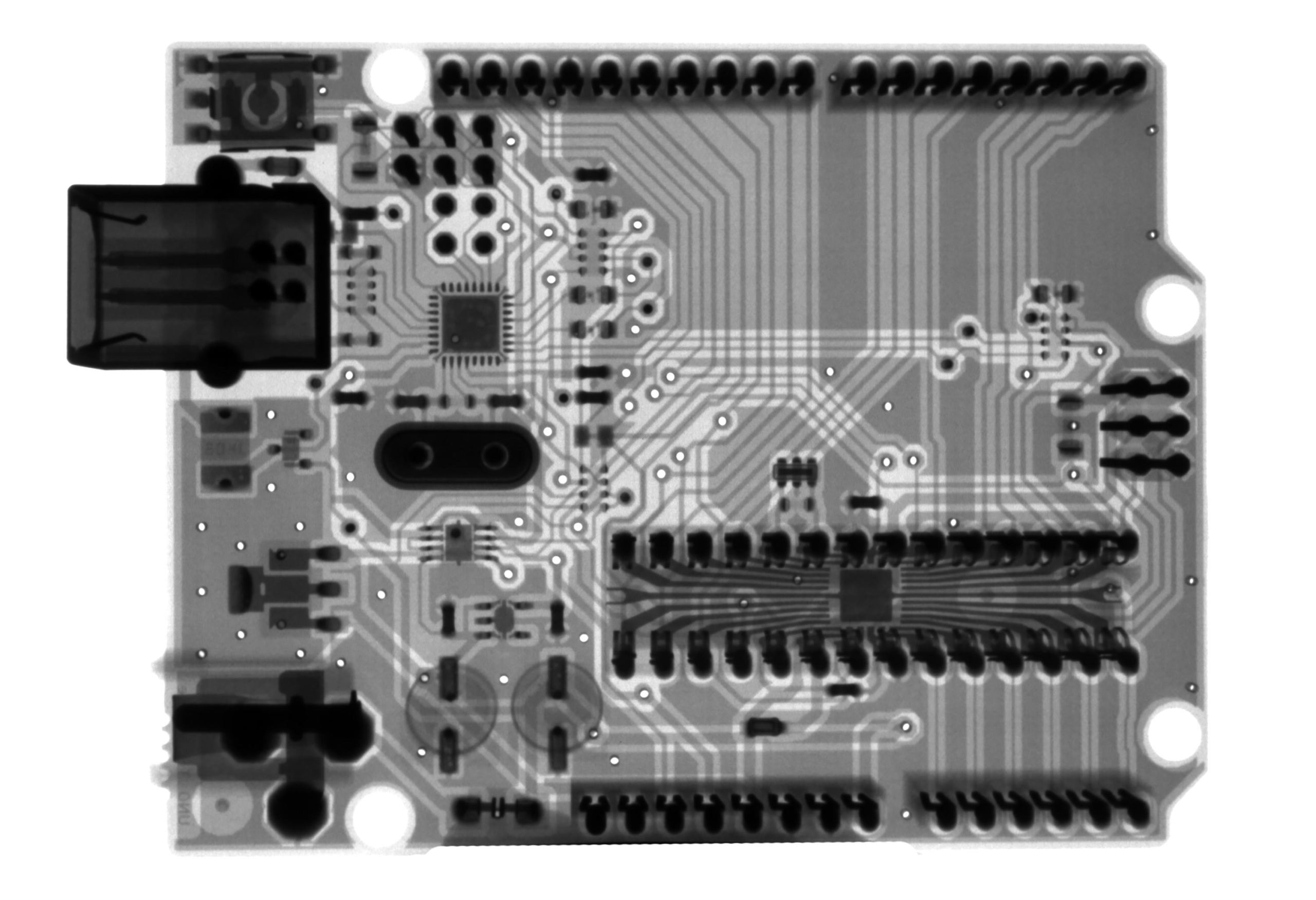
A Printed Circuit Board is a board made of insulating material with circuitry printed on it.

A Printed Circuit Board, or PCB, is a thin board made of plastic or other insulating material. It is used to support and connect electronic components using conductive tracks, pads and other features etched from copper sheets laminated onto it.
PCBs are found in almost all electronic devices, from your cell phone to your computer to your car. They are used to connect and control the various electronic components in these devices.
PCBs can be simple, with just a few components, or complex, with hundreds of components. The number of layers in a PCB also varies, from one to several.
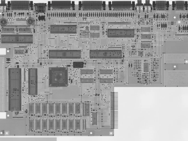
Here is a simple example of a PCB:
This PCB has just two layers of copper. The top layer is the “trace” layer, where the conductive tracks are etched. The bottom layer is the “plane” layer, where the ground or power planes are located.
In between the two layers is a thin layer of insulation, called the “core”. This is typically made of FR-4, a glass-reinforced epoxy laminate.
The copper tracks on the trace layer are connected to the various components on the PCB using “vias”. These are small holes that are drilled through the PCB. They are then filled with copper and connected to the tracks on the other layer.
The tracks on the PCB are connected to the components using either “solder pads” or “plated-through holes”. Solder pads are simply copper pads that the component’s leads are soldered to. Plated-through holes are holes that go all the way through the PCB, with copper on the inside of the hole connecting the tracks on the different layers.
PCBs can be made using a variety of methods, but the most common is “photo-lithography”. This is where a photographic film is used to transfer the image of the tracks and other features onto the copper sheets.
Once the tracks are etched onto the copper sheets, they are laminated onto the core material. The whole assembly is then cut to size and the holes are drilled.
The PCB is then “populated” with the components. This is where the components are placed on the PCB and soldered in place.
Once the components are soldered in place, the PCB is then “tested” to make sure it is working correctly.
PCBs are an essential part of electronic devices. They provide the support and connection for the electronic components. They are made using a variety of methods, but the most common is photo-lithography.
What Is A PCB Layout?
A PCB Layout is a plan for the physical layout of a printed circuit board.
PCB layout is the arrangement of components and tracks on a printed circuit board (PCB). It is also known as PCB design.
A PCB layout is created for each layer of a PCB. The layout includes all the elements that will be printed on that layer. This includes the tracks, components, vias, and text.
The components are placed on the layout according to their function and connectivity. The tracks are then routed between the components. The tracks must not cross each other, and they must not touch any of the components.
Vias are used to connect the tracks on different layers. They are placed at the intersections of the tracks.
The layout is then sent to a PCB manufacturer, who will print the layout on the PCB.
PCB layout is a critical part of PCB design. It must be done carefully to ensure that the tracks are routed properly and that the components are placed correctly.
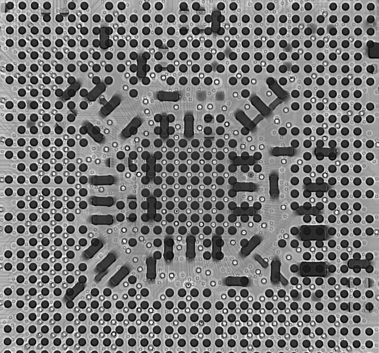
Here is an example of a simple PCB layout:
This layout has two tracks. One track goes from the power supply to the LED. The other track goes from the switch to the LED. The tracks are routed around the components.
The tracks are not crossed, and they do not touch any of the components.
The vias are placed at the intersections of the tracks.
This layout is ready to be sent to a PCB manufacturer.
What Are The Benefits Of A PCB Layout?
Some benefits of a PCB layout are that it can help to improve the performance of a circuit, make it easier to manufacture, and make it more reliable.
When it comes to printed circuit boards (PCBs), the layout is everything. It is the design and configuration of the PCB that will determine how well it functions. A good PCB layout can make the difference between a product that works well and one that doesn’t work at all.
There are many benefits to a good PCB layout. Here are just a few:
1. Improved Electrical Performance
A well-designed PCB layout can improve the electrical performance of a circuit board. This is because the layout can affect the impedance of the circuit board. Impedance is a measure of the opposition to the flow of electrical current. A lower impedance means that less electrical current is required to flow through the circuit board. This can lead to improved performance and lower power consumption.
2. Reduced Electromagnetic Interference
Another benefit of a good PCB layout is that it can reduce the amount of electromagnetic interference (EMI) that is emitted from the circuit board. EMI is a type of interference that can disrupt the operation of electronic devices. It can cause problems such as data loss, system crashes, and hardware damage. A good PCB layout can help to reduce the amount of EMI that is emitted from the circuit board.
3. Improved Thermal Performance
Another benefit of a good PCB layout is that it can improve the thermal performance of the circuit board. The layout of the PCB can affect the way heat is dissipated from the circuit board. A good layout can help to improve the cooling of the circuit board and prevent overheating.
4. Reduced Component Count
A good PCB layout can also help to reduce the number of components that are required to build the circuit board. This can lead to reduced costs and improved manufacturing efficiency.
5. Increased Reliability
A well-designed PCB layout can also increase the reliability of the circuit board. A good layout can help to reduce the likelihood of electrical shorts and open circuits. This can improve the stability of the circuit board and prevent failures.
A good PCB layout is essential for the proper functioning of a circuit board. There are many benefits to a good layout, including improved electrical performance, reduced EMI, improved thermal performance, reduced component count, and increased reliability.
How Does A PCB Layout Improve The Function Of A Printed Circuit Board?
A PCB Layout improves the function of a Printed Circuit Board by allowing for the correct placement of components and routing of traces.
How does a PCB Layout improve the function of a Printed Circuit Board?
It is important to have a well-designed PCB layout to improve the function of a Printed Circuit Board (PCB). A good layout can minimize the circuit board size, reduce the cost, and improve the reliability and performance of the PCB.
There are a few things to consider when designing a PCB layout:
1. The PCB should be designed to minimize the length of the traces. Longer traces are more likely to cause signal integrity problems.
2. The PCB layout should be designed to minimize the number of vias. Vias are required to connect different layers of the PCB, but they can add cost and complexity to the PCB.
3. The PCB should be designed to minimize the use of ground planes. Ground planes are necessary to provide a low-impedance return path for signals, but they can increase the cost of the PCB.
4. The PCB layout should be designed for manufacturability. The layout should be designed so that the PCB can be easily manufactured.
5. The PCB layout should be designed for testability. The layout should be designed so that the PCB can be easily tested.
A well-designed PCB layout can improve the function of a PCB by reducing the length of the traces, minimizing the number of vias, minimizing the use of ground planes, and making the PCB easier to manufacture and test.
What Are The Guidelines For Designing A PCB Layout?
There are no hard and fast rules for designing a PCB Layout, but there are some general guidelines that can be followed to ensure a successful outcome.
Nowadays, Printed Circuit Boards (PCBs) are used in almost every electronic device. They are used to electrically connect and support various electronic components. A PCB layout is a critical part of the manufacturing process as it determines how the components will be arranged on the board. There are various guidelines that need to be followed while designing a PCB layout.
The first thing that needs to be considered is the size of the PCB. It should be big enough to accommodate all the components. The next thing to consider is the shape of the PCB. The most common shapes are rectangular, circular, and oval.
Then, the tracks need to be designed. The tracks are the copper pathways that connect the different components on the PCB. They need to be designed in such a way that they don’t cross each other.
After the tracks, the vias need to be placed. Vias are the connections between the different layers of the PCB. They need to be placed carefully so that they don’t short circuit the tracks.
The next thing to consider is the placement of the components. The components should be placed so that they don’t interfere with each other. They should also be placed so that the tracks can be routed easily.
Finally, the PCB layout needs to be tested. This can be done by using simulation software. This will help to find any errors in the layout.
These are the guidelines that need to be followed while designing a PCB layout.
FAQ
How Can I Ensure My PCB Layout Is Effective?
– Make sure to use an appropriate grid size for the components and tracks.
– Follow the design guidelines for trace widths and spacing.
– Use vias and ground planes to minimize the effects of noise and crosstalk.
– Plan the layout so that the critical signals have the shortest possible path.
– Use test points and access holes as needed to facilitate debugging and testing.
What Are The Common Mistakes Made In PCB Layout Design?
1. Not using proper routing techniques – This can lead to signal integrity issues and crosstalk.
2. Not following the manufacturer’s guidelines – This can lead to issues with the PCB not functioning properly.
3. Not considering thermal issues – This can lead to the PCB overheating and potentially causing damage.
4. Not using proper grounding techniques – This can lead to electrical noise and interference.
5. Not using proper shielding techniques – This can lead to electromagnetic interference (EMI).
How Do I Avoid Making Mistakes In My PCB Layout Design?
1. Use a professional PCB layout design software package, such as Altium Designer.
2. Follow best practices for PCB layout design, such as those outlined in the IPC-2221 standard.
3. Work with an experienced PCB layout designer, if possible.
4. Make sure to check your design for errors before sending it to fabrication.
Conclusion
A PCB layout is the organization of components on a printed circuit board.
Hopefully, you are clear on what PCB layout is. If you still have any questions, feel free to comment below.