Schematic capture is the process of designing a circuit using a graphical representation of the electronic components.
Schematic capture is the process of converting a circuit diagram into a format that can be used by electronic design automation (EDA) software to create the layout for a printed circuit board (PCB). The most common format for schematic capture is the Electronic Design Interchange Format (EDIF), which is a text-based format that can be read by a variety of EDA software.
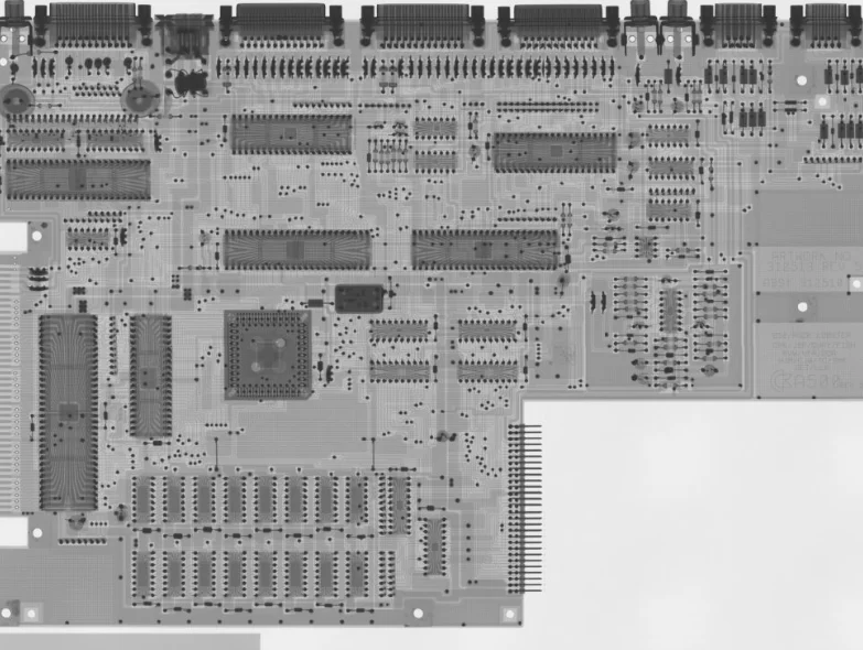
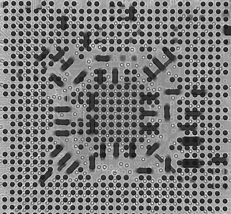
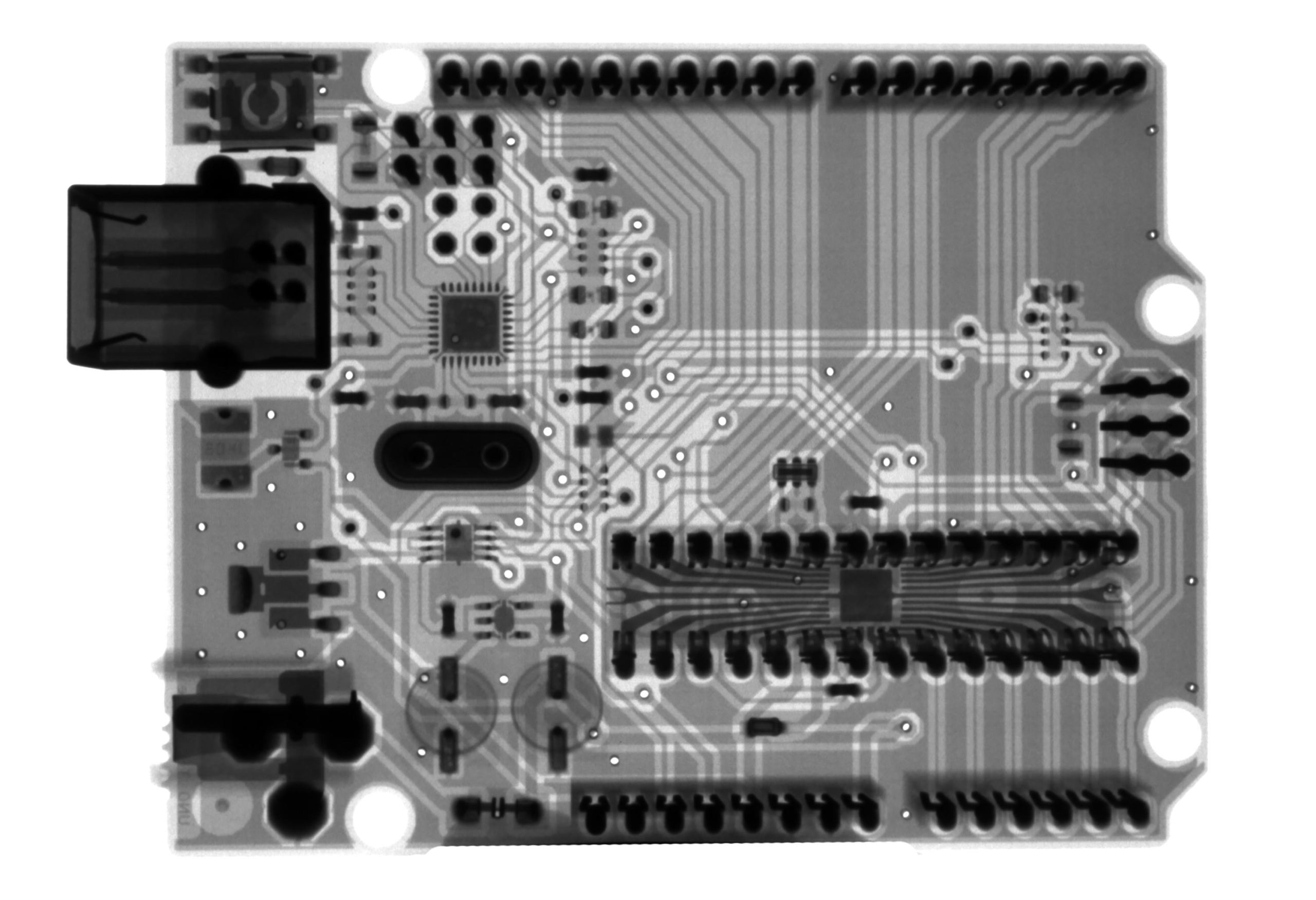
PCB layout is the process of creating the physical layout of a circuit board. This includes placement of the components on the board, routing of the traces between the components, and creation of the solder mask and silkscreen layers. PCB layout is typically done using EDA software, which can automatically place and route the components based on the input from the schematic capture step.
What Is The Purpose Of Schematic Capture?
The purpose of schematic capture is to create a graphical representation of an electronic circuit.

In the field of electrical engineering, schematic capture is the process of converting a circuit diagram into a format that can be simulated by computer. This is done by first tracing out the circuit by hand, then entering the tracing data into a computer program. The computer program then uses the data to generate a schematic diagram of the circuit.
The purpose of schematic capture is to allow electrical engineers to design and test circuits before they are built. By simulating the circuit in a computer program, engineers can find errors and optimize the design. Schematic capture is also used to create PCB layouts.
In the past, schematic capture was done by hand, but today it is mostly done with computer programs. There are many different software programs available for schematic capture, each with its own advantages and disadvantages.
One of the most popular schematic capture programs is Eagle. Eagle is a free, open-source program that runs on Windows, Mac, and Linux. It has a simple user interface and a wide range of features. Another popular program is KiCad, which is also free and open-source. KiCad runs on Windows, Mac, and Linux. It has a more complex user interface than Eagle but is still relatively easy to use.
What Is The Difference Between Schematic Capture And PCB Layout?
Schematic capture is the process of designing a circuit using a graphical representation of its components and connections, while PCB layout is the process of arranging those components and connections on a physical board.
Schematic capture and PCB layout are two important steps in the design of an electronic circuit. Schematic capture is the process of creating a schematic diagram of the circuit, which is a graphical representation of the components and their interconnections. PCB layout is the process of creating the physical layout of the circuit on a PCB.
The main difference between schematic capture and PCB layout is that schematic capture is a design step that creates a schematic diagram of the circuit, while PCB layout is a manufacturing step that creates the physical layout of the circuit on a PCB. Schematic capture is done using circuit design software, while PCB layout is done using PCB design software.
Another difference between schematic capture and PCB layout is that the schematic diagram is a logical representation of the circuit, while the PCB layout is a physical representation of the circuit. The schematic diagram does not show the physical placement of the components, while the PCB layout shows the physical placement of the components.
Here is a real-life example of the difference between schematic capture and PCB layout. Suppose you are designing a circuit that will be built on a PCB. You will first need to create a schematic diagram of the circuit using circuit design software. This schematic diagram will show the components and their interconnections. Once the schematic diagram is complete, you will then need to create the PCB layout. This will involve placing the components on the PCB and routing the tracks between the component pads.
What Are The Benefits Of Using A Schematic Capture Tool?
The benefits of using a schematic capture tool are that it can save time and improve accuracy.
Schematic capture tools are used to create electronic circuit diagrams. They allow you to design and test circuits before you build them, which can save you time and money.
There are many benefits to using a schematic capture tool. For one, it can help you check your work for errors before you build the circuit. This can save you time and money, as you won’t have to rebuild the entire circuit if there is a mistake.
Another benefit is that you can test the circuit before you build it. This can help you find any problems with the design, and fix them before you start soldering.
Overall, using a schematic capture tool can save you time and money, and help you create better circuits.
How Does Schematic Capture Help In The PCB Design Process?
Schematic capture helps in the PCB design process by allowing the designer to create a schematic of the PCB, which can be used to verify the correctness of the PCB layout.
Schematic capture is the first step in the PCB design process. It is the process of creating a schematic diagram of the circuit. This diagram is then used to generate the PCB layout.
Schematic capture helps in the PCB design process by providing a clear and concise diagram of the circuit. This diagram can be used to generate the PCB layout.
For example, consider a circuit with two resistors and a capacitor. The schematic capture would show the two resistors and the capacitor connected in series. This diagram can then be used to generate the PCB layout.
The PCB layout would show the two resistors and the capacitor connected in series. This layout can then be used to generate the circuit.
Schematic capture is a vital step in the PCB design process. It helps in the PCB design process by providing a clear and concise diagram of the circuit.
What Are The Features Of A Good Schematic Capture Tool?
The features of a good schematic capture tool are: the ability to create and edit electrical schematics; a library of electrical components; and a set of tools for drawing and editing schematics.
There are many features to consider when choosing a schematic capture tool for your PCB design needs. Below is a list of the must-have features for any good schematic capture tool, along with a real-life example of each.
1. Ease of use: The schematic capture tool should be easy to use, with a user-friendly interface.
2. Flexibility: The tool should be flexible, so that it can be used for a variety of PCB design needs.
3. Accuracy: The tool must be accurate, so that your schematic designs are error-free.
4. Compatibility: The tool should be compatible with other design software, so that you can easily transfer your designs to the PCB layout stage.
5. Cost: The tool should be cost-effective, so that it fits within your budget.
Now that you know the must-have features of a good schematic capture tool, let’s take a look at a real-life example. Altium Designer is a schematic capture tool that has all of the features listed above, and more. With its user-friendly interface and powerful design features, Altium Designer is the perfect tool for your PCB design needs.
FAQ
How Can Schematic Capture Improve The Quality Of PCB Designs?
What Is The Importance Of Proper PCB Layout?
How Can Schematic Capture And PCB Layout Be Used Together To Improve The Design Process?
What Are Some Tips For Creating Successful PCB Designs?
1. Make sure your traces are the correct width for the current they will be carrying. Too narrow and they will overheat, too wide and you’ll be wasting space and materials.
2. Make sure your traces are well-isolated from each other. You don’t want any accidental shorts or crosstalk between signals.
3. Follow the manufacturer’s recommendations for minimum trace widths and clearances.
4. Pay attention to your layer stackup. You want to make sure you have enough layers for all the signals and planes you need, but not more than you need (which would be a waste).
5. Make sure you have adequate power and ground connectivity. You don’t want your power supplies dropping out due to lack of connectivity.
6. When in doubt, consult a professional. PCB design can be complex, and it’s always better to get a second opinion (or even a third or fourth) before committing to a design.
How Can Schematic Capture And PCB Layout Be Used To Improve The Manufacturability Of PCB Designs?
Do you now understand what schematic capture and PCB layout are? If not, please let us know in the comments section below.