Transparent Flex PCB Design & Capabilities


Transparent Flex PCB
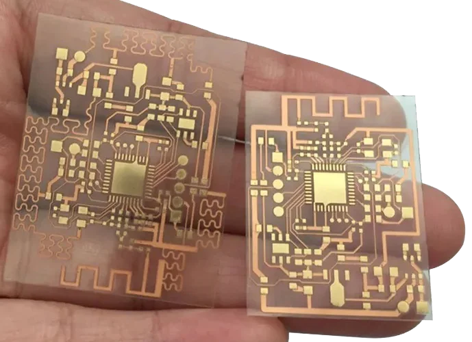
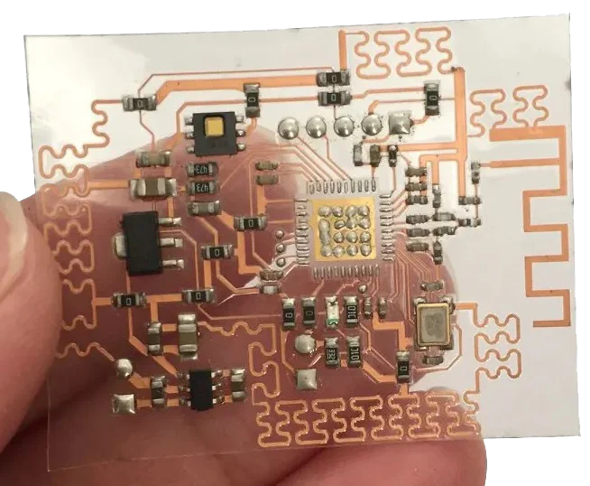
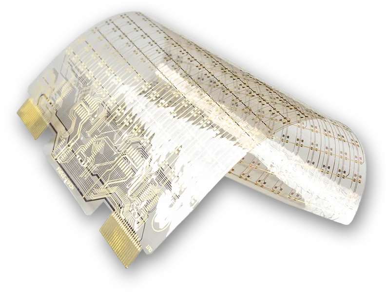
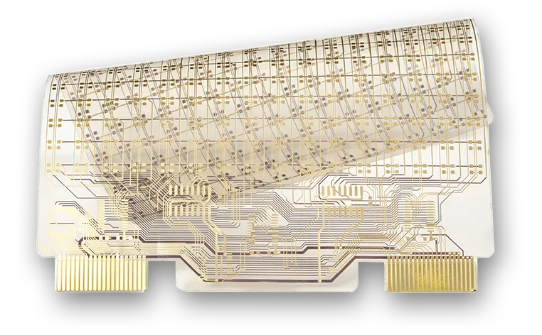
This type of Transparent PCB can be referred to as Clear Flexible PCB that made of PET thin film or Clear polyimide. The PET materials can either be white, transparent, light green, light blue or white. Clear or Transparent flexible PCBs are usually different from the normally seen types.
There are flexible PCBs, where just the substrate is transparent but the pads and conductive traces are not transparent. An innovative method of manufacturing is utilized in making this type PCBs. In this case, the circuit is always clamped in-between two materials (transparent), to help protect it, thereby making it invisible when checked from outside.
Hiberxen offers a comprehensive range of Flexible Transparent PCB designing, manufacturing and PCB assembly.
Advantages of Transparent Flex PCBs
Below are some benefits of the flexible type of transparent PCBs.
- The Transparent flex PCB comes with lots of great optical features
- These are flexible, twistable, foldable, arbitrarily movable and bendable in three dimensions space.
- Achieves thinning, miniaturization and lightness of products.
- These transparent PCB’s manufacturing accurateness reaches the nano or micro level.
Transparent Flexible PCB Applications
The transparent flexible circuit boards are applicable in the following areas.
- Flexible transparent PCBs are widely utilized in ABS systems, mobile phones, cameras, instrument panels, automatic control, medical devices and places where connections are needed in spaces that are closely packed.
- Flexible transparent PCBs that are fully transparent can be utilized in electronic devices, contact lenses, as well as electronic skins.
Transparent Flex PCB Capabilities
| Item | Description | Remark | |
| Layer | Flex board : 1 – 4 Layers | ||
| Material | PI, PET, PEN, FR-4 | ||
| Final Thickness | Flex board : 0.002″ – 0.1″ (0.05 – 2.5mm) | ||
| Surface Treatment | Lead-free : ENG Gold, OSP, Immersion silver, Immersion Tin | ||
| Max / Min Board Size | Min : 0.2″x0.3″ Max : 20.5″x13″ | ||
| Min Trace Width / Min Clearance | Inner : 0.5oz: 4/4mil 1oz: 5/5mil 2oz: 5/7mil | Outer : 1/3oz-0.5oz: 4/4mil 1oz: 5/5mil 2oz: 5/7mi | |
| Min Hole Ring | Inner : 0.5oz: 4mil 1oz: 5mil 2oz: 7mil | Outer : 1/3oz-0.5oz: 4mil 1oz: 5mil 2oz: 7mil | |
| Copper Thickness | 1 / 3oz – 2oz | ||
| Max / Min Insulation Thickness | 2mil / 0.5mil (50um / 12.7um) | ||
| Min Hole Size and Tolerance | Min hole : 8mil Tolerance : PTH±3mil, NPTH±2mil | ||
| Min Slot | 24mil x 35mil (0.6×0.9mm) | ||
| Solder Mask Alignment Tolerance | ±3mil | ||
| Silkscreen Alignment Tolerance | ±6mil | ||
| Silkscreen Line Width | 5mil | ||
| Gold Plating | Nickel : 100u” – 200u” | Gold : 1u”-4u” | |
| Immersion Nickel / Gold | Nickel : 100u” – 200u” | Gold : 1u”-5u” | |
| Immersion Silver | Silver : 6u” – 12u” | ||
| OSP | Film : 8u” – 20u” | ||
| Test Voltage | Testing Fixture : 50-300V | ||
| Profile Tolerance of Punch | Accurate mould : ±2mil | ||
| Ordinary mould : ±4mil | |||
| Knife mould : ±8mil | |||
| Hand-Cut : ±15mil | |||
We're here to help
Our team is ready for you. Feel free to contact us by e-mail or our social media, so we can learn more about you and your needs.
