We Produce Printed Circuit Boards in Every Quality within Global Standard

PCB Fabrication

PCB Fabrication Services

Any electronic product would not be complete without PCB fabrication process after a valid PCB design. For your end product, it is a challenge to find proper quality PCBs and interconnect solutions in competitive price.

With over 12 years of experience in PCB technology, design optimization and manufacturing capability, our PCB professionals will provide you the most innovative and cost-effective solutions for your front-end design through mass production.

Competitive Pricing:
Our experienced PCB engineers works closely with our manufacturing partners to offer the most competitive price while ensuring that PCBs are built following global quality standard. Using extensive knowledge of industry requirements and specifications our PCB team will also assist with design and engineering specifications to improve manufacturability and help identify cost reduction opportunities.

From starting to delivery of your project, we focus on providing the best quality and service. Our experienced staffs and technical support engineers are always ready to ensure that all the needs are met to keep you ahead of your competition.

Process We Follow:

  • RFQ or Sample or First Article Inspection
  • Design for Manufacturing (DFM) Review
  • Check Plot Review/Approvals
  • Production Purchase Order Management
  • Schedule Changes and Expedites
  • Logistics Coordination
  • Quality Commitment
  • PCB Design Optimization, Manufacturing and Quality Assurance Solutions

Advanced Technologies for PCB Solutions

From standard technology to complex, advanced high-density circuits incorporating the latest technology, We will always keep you up-to-date with cutting edge advancement available in the current market.

PCB Types :

  • Standard Single-Sided Rigid PCBs
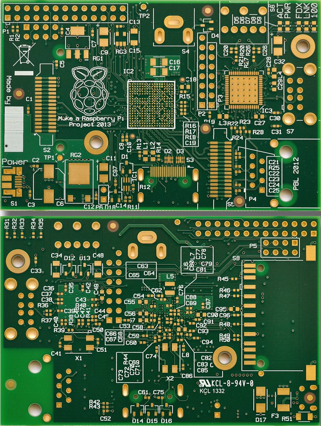
    One layer designs to support thru hole and surface mount.
  • Standard Double-Sided Rigid PCBs
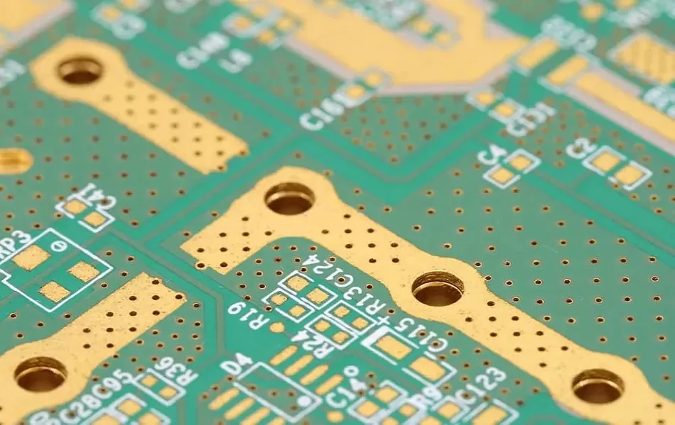
    Mixed technology circuit supporting SMT and thru hole.
  • Multi-layer Rigid PCBs
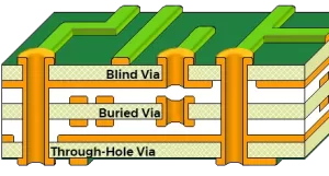
    Up to 32 layer PCBs for High speed advanced designs.
  • Rigid PCB with buried via holes and blind via holes
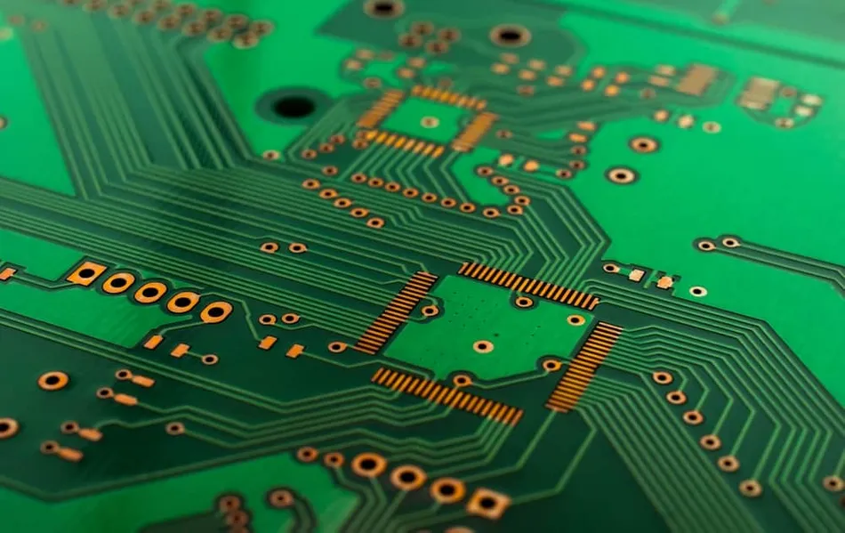
  • HDI Rigid PCB
    High Density Interconnect using laser drilled microvias up to with 1+n+1/2+n+2/3+n+3/4-N-4/ELIC structure.
  • High-frequency RF PCBs
  • Semi-flex PCBs
  • Flexible PCBs
  • Rigid-flex PCBs
  • Aluminum/Thermal PCBs
  • Metal Core (Copper, Ceramic and steel based) PCBs
  • Heavy Copper and Bondable PCBs
  • Ceramic PCBs

Capabilities

Wide range of PCB design and manufacturing Capabilities as follows:

  • Rapid Prototyping and Mass Production
  • Rigid PCBs from 1 to 32 layers
  • Flexible PCBs from 1 to 8 layers
  • High-Density Interconnect (HDI) PCB from 4 to 20 layers
  • Rigid-Flex from 4 to 16 layers with laser drills
  • Controlled Impedance: +/-8%
  • Thin laminate capability down to 2 mil
  • PCB Plating:
    HAL, Lead-free HAL, Flash gold, ENIG, ENEPIG, Gold Finger Plating, Selective Gold Plating, Entek, Immersion Tin, Silver Surface finish. 
    Silver ink through holes, Silver and Carbon ink jumper, Carbon printing.
  • Materials:
    CEM-1, CEM-3, FR-1, FR-2, FR-4, FR-5 (High Tg), High Tg Material (Tg = 180º C), BT, Rogers, Panasonic, ISOLA, Polyamide, Aluminum, Copper, Steel and Ceramic.
  • Finished board thickness:
    0.25 mm / 0.010 inch to 7.0 mm / 0.275 inch.
    Copper thickness up to 10 oz.
  • Hole size:
    0.1 mm/0.004 inch minimum for laser vias, and 0.15 mm/0.006 minimum for mechanic drilling.
  • Trace size:
    0.076 mm/0.003 inch minimum for conventional PCBs, 0.05mm/0.002 minimum for HDI/ELIC.
  • Trace spacing:
    0.076 mm/0.003 inch minimum for conventional PCBs, 0.05mm/0.002 minimum for HDI/ELIC
  • Aspect ratio: 15 : 1 
Immersion Silver (ImAg) PCB
Electroless Nickel Immersion Gold(ENIG) PCB with Gold Finger
Selective Gold Plated PCB

PCB Surface and Finishes

  • Immersion Silver (ImAg)
    Immersion Silver is a good alternative to Electroless Nickel Immersion Gold(ENIG) for fine pitch applications due to the lower cost. This finish is becoming a standard in the industry and works well in lead-free processing. Surface preparation is available in polish or etch, it is important to note that polish should be used for micro technology and etch for all others. NOTE: This finish is not backwards compatible with leaded processing and should NOT be selected for applications which will switch between leaded and lead-free.
  • Electroless Nickel Immersion Gold (ENIG)
    ENIG is a long proven industry standard and is readily available from most PCB fabricators. This finish is suitable for almost any lead-free application regardless of complexity; however is the highest cost finish. This finish is backwards compatible with both leaded and lead-free processing.
  • Immersion Tin
    Immersion tin is a lead-free surface finish, which is excellent for small components. It is very thin and flat and perfect for Fine Pitch Technology (FTP).
  • Flash/Soft Gold
    Soft gold PCB surface finish that is very well suited to wire bonding operations. The soft gold used in this process can easily form strong metallic bonds with standard copper traces and wires. The strong bond of gold and copper allows for more conductive connections when leads are soldered to the board during the PCB Assembly Process.
  • Hard Gold
    Plated Gold surface finish is also known as Hard Gold surface finish. It’s an expensive surface finish that uses a layer of gold on the PCB. It’s done through electroplating, and a hard layer of gold is attached to the surface of the copper. The adhesion between the PCB and the layer is firm, which increases the durability of the board.
  • Palladium
    Electroless Nickel Electroless Palladium Immersion Gold (ENEPIG) is the best surface finish that resists corrosion and reaction with air. It has a longer shelf life, which makes it the best of all.
  • Organic Solderability Preservatives (OSP)
    OSP is one of the PCB surface finishes, means Organic Solderability Preservatives, which is applied upon the bare copper to prevent PCB from being oxidized. OSP is RoHS compliant and can be quickly removed in the PCB assembly processing.
  • Hot Air Solder Leveling (HASL)
    Hot air solder leveling (HASL) is a widely used PCB surface finish. It is inexpensive and easily available. It also offers a high solderability finish, making it a dominant player in the market for several years. Due to the RoHS directive, there is a major transition from HASL to lead-free HASL.
Organic Solderability Preservatives (OSP) PCB
Electroless Nickel Electroless Palladium Immersion Gold (ENEPIG) PCB

Our Projects

Check out the list of services below to find out more about what HiberXen can do for you.

Rigid PCB

Multi-Layer 1 - 32 Layers

Flexible PCB

Multi-Layer 1 - 8 Layers

Flex-Rigid
PCB

Transparent
Flex PCB

HDI PCB

High-Density Interconnect

High-Frequency
or RF PCB

Thick Copper
PCB

Aluminum
PCB

Metal Core
PCB

Ceramic
PCB

We're here to help

Our team is ready for you. Feel free to contact us by e-mail or our social media, so we can learn more about you and your needs.

Scroll to Top